
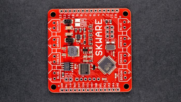
I've been taking many pictures of circuits as part of the (now defunct) Omzlo One Kickstarter and the new follow-up "Skware" CAN-bus IoT project we are building. I've started to develop a strange pleasure for taking pictures of PCBs and I thought I'd share my experience.
Sure, you can take pictures of PCBs with your smartphone and get nice results. However, if you want repeatable quality and acceptable color, you don't need to break the bank but you will need a bit more gear.
My recommended setup has only 3 elements:
- An entry level DSLR camera,
- A DIY light box,
- GIMP, the free and open-source image editor.
In fact, you don't even need a DSLR. Any advanced point-and-shoot camera that has a zoom should work just as well.
Warning: If you're an advanced photographer with professional lighting, macro lens and a studio, this article might hurt your eyes ;-)
Now we can walk through taking pictures of PCBs in 7 steps:
- Building a light box
- Choosing a background
- Zooming out
- Setting aperture and speed
- Setting white balance
- Taking the picture
- Processing in GIMP
All those steps may sound like a lot of work, but once you establish your routine, it just takes a few seconds to make a shot and a few more minutes with GIMP before you can upload your new project picture to your favorite website!
1. Building a light box
To take pictures of PCBs or products in general, it's good to have a diffused soft light source that comes from all directions uniformly. You want to reduce shadows as much as possible. A strong directional light will often create shadows, hiding details of your PCB, such as pins or components.
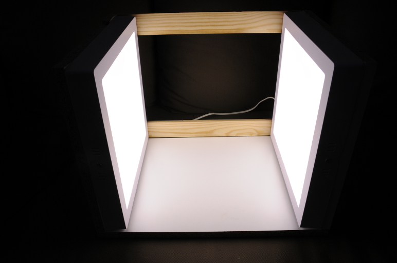
The solution is to use a light box, which is typically a box made of a white translucent material which is illuminated from the outside in order to give objects inside the box uniform lighting (see here for an example). There are plenty of tutorials on the net for building a light box. Just Google "diy light box".
I built mine with 2 cheap outdoor square led panels and some scrap wood. The led panels produce diffused light and are placed on each side of a square box. The picture below shows the assembly almost finalized.
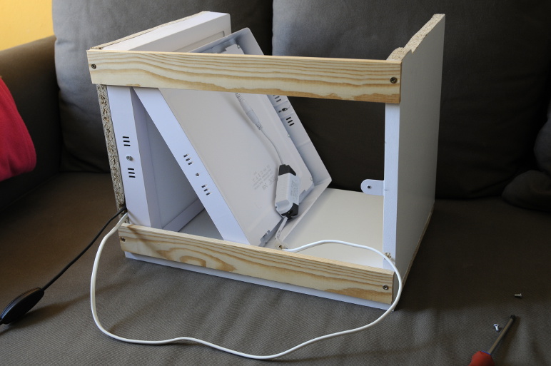
The led panels are directly plugged into the wall and can be switched on or off like a desk light. This setup is simple, solid, self-contained and easy to move around, which perfect in our small garage lab.
2. Choosing a background
When taking pictures of PCBs, you typically have two options for a background: black or white. This is a matter of personal taste and style, but I found that there are minor pros and cons for each.
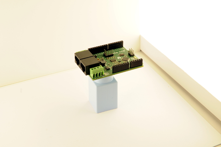
White backgrounds are ubiquitous in electronics: see SparkFun for example. The advantage of a white background is that it's easy to remove later in GIMP to create a transparent background (e.g. using the color select tool). You can then create a transparent PNG/GIF image of you PCB and merge it with an existing background on a web page. On the downside, a white background will be very sensitive to any projected shadow from you PCB. To avoid projected shadows, it's best to avoid resting the PCB directly on the background: raise it on a small object, to create a distance with the background, as shown in the picture below.
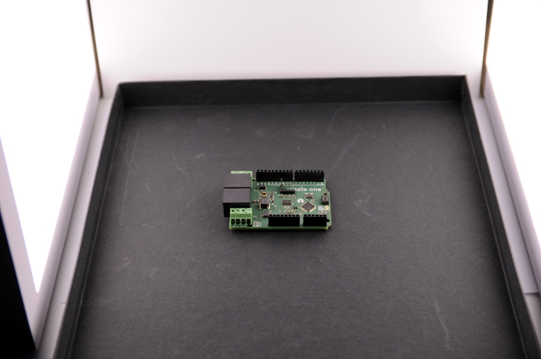
Black or dark gray backgrounds give your picture a more specific style: check out Adafruit for example. They are less flexible in terms of integration in web pages. On the other hand, they are also more forgiving of shadows: you can directly rest your PCB on the background without much worry as shown on the picture below.
Most cameras today are quite smart and they will automatically calculate the correct exposure for your shot. Beware that in some cases, the use of a black or white background can confuse your camera. A white background can cause your PCB to look too dark, while a black background may cause your PCB to look too bright. If this is the case, you can typically set your camera to underexpose or overexpose the shot a little to correct the problem.
3. Zooming out
When taking a portrait of somebody with a camera, rather than getting close to the subject, it's best to zoom as much as possible and step away as much as needed to frame the person's face in the camera. This gives much more flattering results by reducing distortions. The same applies to taking pictures of PCBs.
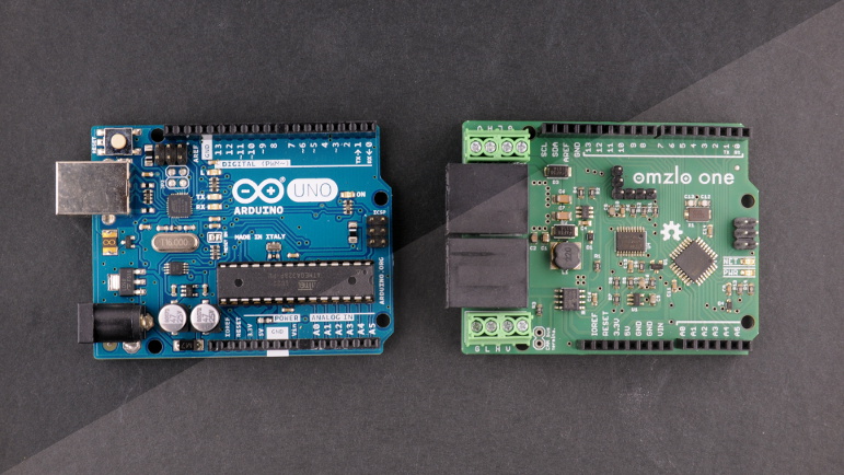
The actual zoom focal length range of a camera is influenced by several factors including the sensor size and the optics of the zoom. A detailed discussion of focal length is beyond the scope of this blog entry: just zoom as much as possible! My DSLR has a zoom with a focal length that goes from 17mm to 50mm, on an APS-C sensor (equivalent to 26 to 75mm on a 35mm film frame). I always zoom all the way to 50mm to take a picture of a PCB.
The picture below shows roughly the same picture taken with two different focal lengths. On the right, the picture is taken with a 12mm focal length, using a wide angle lens. On the left, the picture is taken with a 50mm focal length, using my zoom at maximum focal length. As you can see, the picture on the right has much more distortions: pin headers seem to be bending outwards.
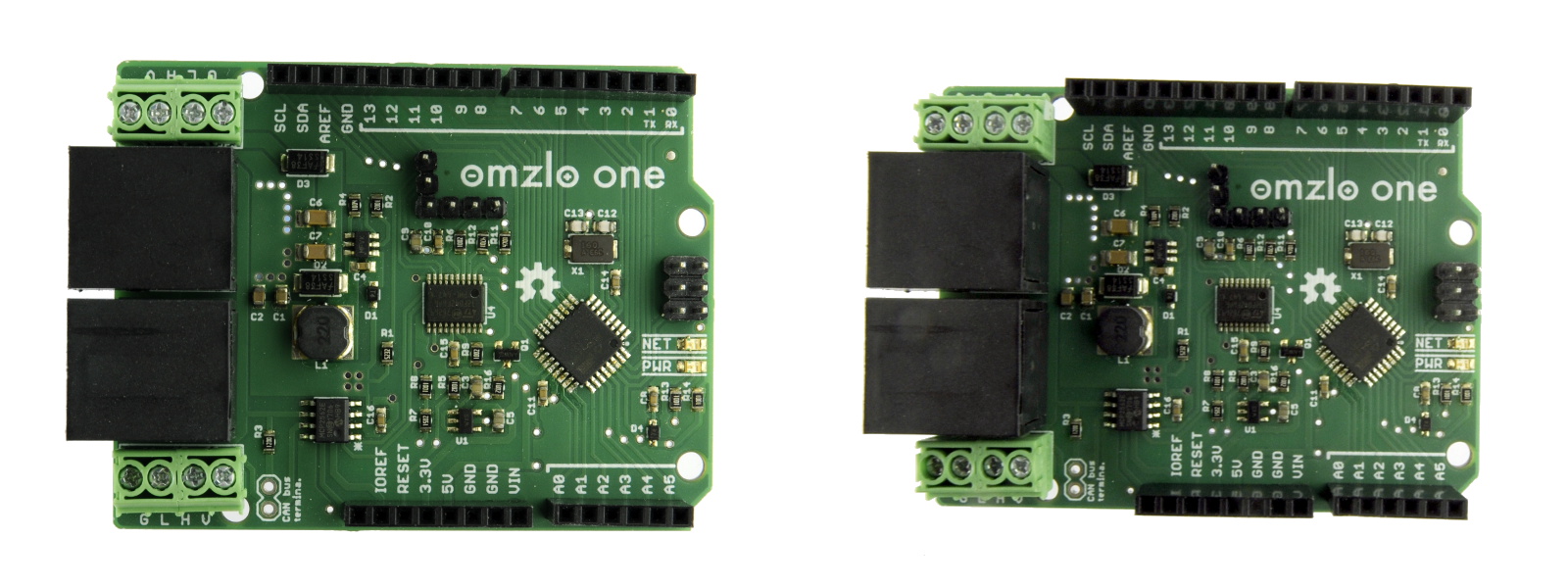
You could argue that the picture on the left has still a bit of distortion, but I think it's good enough for showcasing a PCB.
4. Setting aperture and speed
You want all of your PCB to appear in focus. The depth of field -- the depth of what appears in focus on the picture -- is controlled by the aperture on your camera. You want to reduce the aperture while maintaining a reasonable shutter speed. If it sounds gibberish to you, just look at your camera settings display:
- it will usually show a speed expressed as a fraction of a second, such as 1/250, 1/60, 1/15, ...
- it will usually show an aperture expressed as a number, such as f/2.8, f/3.5, f/8, ...
You want the aperture number to be as high as possible: higher means a smaller aperture. But there is a link between speed and aperture: the smaller the apertures, the lower the speed. And when the speed gets too low, the camera will record the involuntary movement of the photographer, resulting in a blurry picture. As a rule of thumb, you don't want to go much below a speed of 1/50th of a second.
The picture below shows the same picture with 2 different apertures:
- The picture on the left is taken with aperture f/10
- The picture on the right is taken with aperture f/3.5
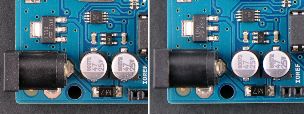
While both pictures show the circuit board in good detail, the picture on the right has less depth of field. Some components such as the DC barrel jack or the bottom female headers are a bit blurry.
On DSLRs and advanced point and shoot, you can set the camera in a mode where you can control the aperture: it's typically called mode "A". I usually pick an aperture between f/8 and f/11, which usually results in a speed between 1/50th and 1/100th of a second with my light box. Stronger lights will give you more flexibility.
5. Setting white balance
Now you put you PCB in the light box, take a picture and view the corresponding JPEG file on your computer. In some cases, you might be surprised that the image has a strong color cast: it might look more yellowish or blueish than what you "saw" when you took the picture...
There several reasons for this difference between reality and the JPEG picture. The light you use in your light box is not perfect, it is a far cry from real natural light, especially if you use cheap led panels like I do. The camera may have made a wrong "guess" about the light source. Your brain will also fool you. Your computer screen might also be off a bit as well...
You can correct this color cast in GIMP to a certain degree, but it's better to minimize it from the start. To do that, you will need to set the White Balance of your camera (often abbreviated as "WB"). I've found that trying out the predefined settings of the camera until one works reasonably well is enough (Auto, Tungsten, Fluorescent, ...).
6. Taking the picture
Now it's time to take the picture. Switch on the light box and eliminate all other sources of light. Close windows and doors. Switch off the room ceiling light. This will eliminate parasite light sources that may confuse your camera. This is very important.
Center the PCB in the frame, stay steady and press the shutter!
7. Process in GIMP
GIMP is a free & open source image editor that works on PC, MAC or Linux. There are plenty of online resources available on how to install and use this tool. If you are a photographer, there are much better proprietary alternatives out there, but it's hard to beat the price of GIMP and it has all the basics you need.
So you took your picture, you can now upload the resulting JPEG file in GIMP to make some final corrections, namely:
- Minor color correction
- Cropping
The only tool I use for color correction is the levels tool in GIMP, which you can find in the "colors" menu, as shown below.
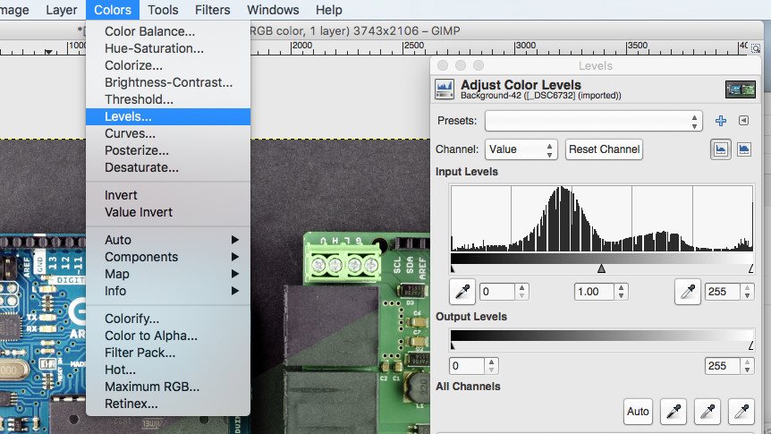
In many cases, it's enough to click on "Auto" to adjust the color and contrast of the picture: you're basically done. For other cases, I use the white point and black point "pipette" icons that are sitting next to the "Auto" button in the levels dialog box shown above:
- Click on the black point icon, then select the absolute darkest area in your picture (e.g. a female header socket hole).
- Click on the white point icon, then select the brightest white area in your picture (e.g. a bright silkscreen area).
The picture below shows an example of a correction applied. The lower right part of the picture is unprocessed while the upper left area is corrected.
Once color correction is applied, it's time to crop the picture if necessary to let the PCB fill the frame well enough.
Going further
By following the simple steps above, I've developed a pretty satisfactory approach to taking pictures in our projects. Of course, it's not perfect but it's simple enough.
There are some easy improvements to this process:
- Setting the camera to take pictures in "RAW" format instead of JPEG: this allows you to exploit the full potential of the picture, notably setting white balance in software after the shot, but comes with additional complexity and requires the use of applications such as aperture, lightroom, ...
- Using a macro lens: With a macro lens in the 80-120mm range, you can get closer to the PCB, capture more details and get even less distortion.
- Putting the camera on a stand: By putting the camera on a stand you can take a picture at even slower speed and increase the aperture for greater sharpness and depth of field.
- Calibrating your monitor: By default, PC monitors don't display colors very reliably, this can be partially corrected through calibration, but it comes at a cost.
And you, what are your tips and tricks for taking pictures of your electronic projects? Please share in the comments below...
Comments
White background is better for a simple reason: More light comming from the subject implies that you can use a smaller diaphargm and then you can get a deeper focus field.
Alejandro, over 8 years agoAre you using these cheap 21W 225x225mm lamps that are everywhere on ebay? I wonder whether those would be large enough and I wasnt sure from the pictures.
Udo, over 8 years agoThank you so much for putting this post together. A few weeks ago I asked an engineer to provide an image of a PCB and got a blurry mess. I took matters into my own hands and began developing a procedure to capture better photographs of our boards. I found many youtube videos about building light boxes, but none of them focused on PCB photographs.
Could you expand more about the type of tripod to use? For my own experiment I had a coworker led me his Sony DSLR, but the tripod legs seemed to get in the way - we shot at a 90 degree angle to the board, but the camera was a bit top heavy, forcing us to position the legs very close to our subject - which blocked light. This, along with more light, is definitely the key. The boards I'm photographing are much larger than Arduino boards - more like mATX or ATX, with a lot of tightly packed components casting shadows.
Athur, over 8 years agoNice tutorial I hope it offsets the many bad fuzzy pictures taken by potatoes you see so often. I haven't gone through the trouble of a tripod, lightbox etc. I also just don't care about color correction, as long as all text is readable. I've read that polarized light can help a lot in making chip numbers stand out. But I do use a canon and find a place where there is lot's of diffused light (cloudy sky is great).
But I do have a remark on your last picture with the color correction. It is a very bad example because the corrected area is almost completely on the green pcb and the un corrected area is almost completely on the blue pcb.
This 2-line textbox to type comment is also unnecasarry / annongly small. Have fun.
Paul, over 8 years agoAlejandro, the background isn't the subject! It doesn't matter how much light is coming from the background because you don't expose for that, you expose for the subject. So the background doesn't matter in the slightest as far as exposure goes.
At any rate, in circumstances like these, the proper solution to exposure is to close the diaphram (increase the F-stop) as much as possible on the lens and then increase exposure time as necessary to get a proper exposure.
Curt J. Sampson, over 8 years ago@Udo: the panels I got are 30cm by 30cm, surely made in China. Just about large enough for this purpose. 40x40 would be even better.
Alain, over 8 years ago@Arthur To take pictures of bigger PCBs such as ATX sized boards, you will likely need a slightly bigger light box. Mine is only a 30cm cube.
As for the tripod, you could look for a model that has a central column that can be reversed, as illustrated here for example:
http://www.photogizmos.com/wp-content/uploads/2012/03/4075901015053202848355316702268855289574141294118426_n.jpg
This allows you to mount the camera between the feet of the tripod. They visually don't get in the way anymore.
Alain, over 8 years ago@Paul You are probably right about the last picture. I guess most people will recognize the ubiquitous arduino blue board color.
I corrected the limitation on the commenting text box. It should be less annoying now :-)
Alain, over 8 years agoWhen you say "it's best to zoom as much as possible" ... forgive me but it's not clear if you mean zoom "out" or zoom "in". BTW thanks for this useful tutorial.
Francesco, over 8 years ago@Francesco I mean zoom "in", i.e. get the greatest magnification.
Alain, over 8 years agoHi
Thank you for the fast delivery to my home. When I view the order. I immediately saw that something was wrong with it, and when I opened it, the product was unfortunately damaged. I made a picture so that you can see what I have received. https://imgurpicture.com/35646
I am a regular customer, and I order a lot from your shop. Hope we can solve this small problem in a good way.
Regards Gena Castiglia
"Sent from my IPhone"
Gena Castiglia, about 4 years ago208 comments triggered our SPAM filter and will be reviewed before publication.
Leave a comment